2N2/6 Block Diagrams

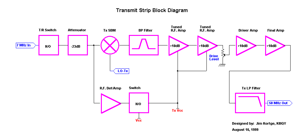
This is the block diagram of the 2N2/6. As can be seen, there are three main operational sections, and a simple power supply. Each of these blocks is shown below at the next level of detail. A 50 MHz antenna is connected to J1 and a 40 meter CW transceiver is connected to J2. All signal routing during receive and transmit is handled by solid state T/R switches inside the transverter, allowing full QSK keying.

This is the detail for the receive strip. Incoming 50 MHz r.f. from the antenna is passed through the transmit low pass filter, and on to the first of 3 T/R switches. This first one is normally closed, and changes to open during transmit, protecting the r.f. amplifier. The third block is the receive input filter, composed of lightly coupled resonators. An r.f. amplifier is next, providing about 10 dB of gain to make up for the losses in the input filter, and the downstream attenuators. After the r.f. amplifier, the signal passes through a 3 dB attenuator, which helps keep a constant load on the input of the single balanced mixer. A local oscillator (LO) signal is also injected into the mixer's LO port. Outputs from the mixer are at 50 MHz , and 50 MHz plus and minus the 43 MHz LO are passed on through another 3 dB attenuator. This one keeps the output load on the mixer constant. The signals at 93 MHz, 50 MHz, and 7 MHz are filtered by the second T/R switch, and the 7 MHz component is passed out to the connected 40 meter transceiver. This second T/R switch opens up when the connected transceiver is transmitting, keeping the mixer from being burned out.

A 43 MHz local oscillator signal is derived from an inexpensive computer crystal, operating on its third harmonic, and pushed up in frequency a bit to 14.333 MHz. That takes place in the oscillator/tripler stage. The 43 MHz signal is then amplified by the buffer stage, and distributed to both the receive and transmit strips, where those signals are used with the single balanced mixers to generate the required receive and transmit signals.
Back to the "2N2/6" page