The amplifier has an input impedance of 50 ohms, and an output impedance of 0.5 ohms, making it an almost perfect voltage source. While the Manhattan-style construction version would make a most useful utility amplifier, one could lay out a PC board for the design and by using SMT components, create a very small amplifier module to fit on an existing DDS card or for other uses. Follow this link to see an implementation of this idea by Dave Rogers, WB4CHK.
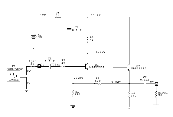
This is the schematic diagram of the
amplifier. It is slightly different than the version I was showing earlier
both in component values and other features. This is actually the circuit
modeling schematic from CircuitMaker (TM). Included on this schematic are
the dc bias values at each circuit node.
Other transistors can be used, such as MPSH10s if higher frequency response is required. PN2222 transistors will work fine out to about 30 MHz. A small inductor can be added in series with the 620 Ohm resistor to improve frequency response flatness. SPICE modeling is recommended to optimize the inductor value.
Other transistors can be used, such as MPSH10s if higher frequency response is required. PN2222 transistors will work fine out to about 30 MHz. A small inductor can be added in series with the 620 Ohm resistor to improve frequency response flatness. SPICE modeling is recommended to optimize the inductor value.

This is the Bode, or frequency response plot for the circuit above. The yellow trace is the output, and the green plot is the input. These are points "A" and "B" shown on the schematic.

A transient response plot from the simulation. The yellow trace is the output, and the green trace the input with the generator set for 100 millivolts peak-to-peak.

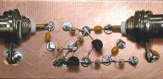
The amplifier was build Manhattan-style on a small substrate. The input is on the left BNC, and the output is on the right BNC. Power is applied to the upright pin just to the left of the output BNC ground lug and the ground lug itself.

Looking toward the output BNC from the opposite side. The +Vcc power pin can now be seen clearly.
An overhead view showing the pad locations for those who want to try building their own version. For reference, the substrate is 1 1/4 inches wide, and 2 1/8 inches between the two BNC ground lugs. Node pads are 1/8 inch in diameter.

This is a frequency response or Bode plot of the "as built" amplifier. The signal input is at -30 dBm and the output amplitude is as shown.
The small amount of droop at 30 MHz could be removed with a 1.5 to 1.8 uH molded inductor in series with the 620 Ohm feedback resistor.
Back to "Miscellaneous" page