As many of you know, measuring most receiver parameters requires using two sources, usually offset by 5, 10 or 20 Khz. While one might have a good signal generating source in the lab, having two of them is often prohibitive from a cost stand point. This -20 dBm source can be built for any frequency. However, for my use in measuring the receive strip of my new 2N2/20 transceiver, a second signal source on 20 meters was needed. Since readily available crystals are available from NorCal, and other suppliers, that hardest-to-find of the parts is quite easy to acquire.
This source can be used in many ways. When used with a precision attenuator, one can measure a receiver's Minimum Discernable Signal, or MDS. Another measurement that can be made with this combination is opposite sideband supression or rejection.
When used with another signal generator having an adjustable output level, and a 3 dB splitter/combiner, one can measure the other parameters that characterize receiver performance such as Blocking Dynamic Range, Intermod Dynamic Range, and 2nd and 3rd Order Intercept points. Details of how to perform these measurements can be found on the ARRL web site, and in numerous technical journals.
Three attributes are important in a signal source used for receiver measurements. They include: frequency stability, amplitude accuracy, and signal purity. The circuit used for this source provides two of the three, and the packaging approach provides the remainder. Frequency stability is achieved through the use of a crystal and operating the crystal at a very low excitation level. This approach minimizes crystal heating, and heating within the feedback capacitors and other circuit components. The crystal itself provides most of the frequency stability. However, crystal heating detracts from frequency stability. Capacitor heating primarily affects amplitude (output level) accuracy. Signal purity is assured by extensive shielding of the active circuitry in the top part of the housing, and also minimizing leakage into the housing by outside sources, such as nearby commercial radio stations. The shielding provided by the enclosure design is on the order of 100 dB.
The circuit itself is a common Colpitts configuration, but with some important changes over the circuits one normally sees. First is the collector supply, which is regulated at a very low value, using a 1.8 volt LED. This is the first step in assuring low power circuit operation. The second circuit change is the use of a large emitter resistor, 3.9K, to limit circuit current. These two circuit features, along with relatively small feedback capacitors, provide the required frequency stability and amplitude accuracy desired. The output impedance of the source is 51 ohms, determined by the collector resistor. A 3-pole, half wave output filter removes harmonic content, so that the output purity is acceptable. Spurious signals are -35 dBc or greater.
The same topology can be used for building a signal source on other ham bands, or any frequency for which a crystal is available.
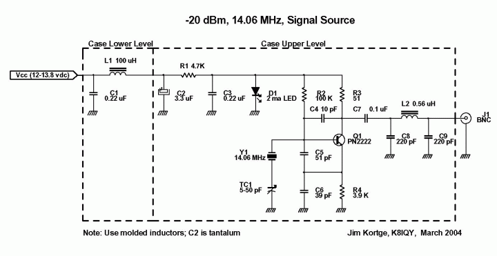
Here is the schematic for the -20 dBm signal source. Starting from the left, the supply voltage is filtered with the C1, L1, and C2 components. From there, R1 limits the current available to D1, the 2 ma LED. It operates as a low voltage Zener diode, to keep the voltage going to Q1 at 1.8 volts. Q1 is configured as a Colpitts oscillator, running very low collector current by virtue of base bias resistor R2, and R4, the 3.9K emitter resistor. Output is taken from collector resistor R3, selected to provide the desired 50 ohm output impedance. Components C8, L2, and C9 provide output filtering to smooth the wave form, and significantly reduce 2nd and 3rd harmonics.
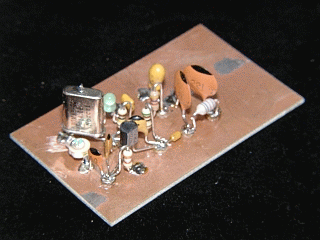
This project was built Manhattan-style, as is just about everything I do. The single sided PC board substrate was larger than needed during building. It was later cut down to size using a small shear, obtained from one of many online tool supply houses. The final size is 1.5 inches by 2.5 inches.
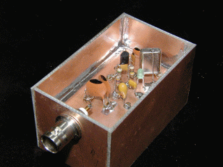
Pieces of double sided PC board material were cut to size using the shear, and soldered around the perimeter to form a box structure. With this approach, no RF can leak out and contaminate the measurements being made, nor can strong external RF sources get in.
The power supply lead was routed through a hole in the substrate to the bottom of the board. This bit of circuitry is the coaxial power connector, and the components used to keep RF from leaking out of the box on the power supply lead.
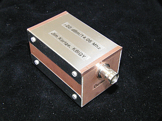
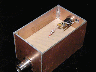
Top and bottom covers were bent out of tin plated stock obtained from a hobby shop and screwed in place. Adhesive backed copper tape was then used to cover the small gaps at the cover ends that might let small amounts of RF leak out. Small rubber feet on the bottom and some simple labeling completed the project.
Back to "Test Equipment" page