2N2/6 Construction Pictures

A first picture showing the 2N2/6 receive strip. The input filter is on the rightmost side, followed by a tuned output r.f. amplifier, -3 dB attenuator, trifilar wound toroid for single balanced mixer, another -3 dB attenuator, and output T/R switch. The r.f. amplifier was later redesigned and rebuilt to make it more stable.

This picture shows the rebuilt r.f. amplifier, and the first configuration of the local oscillator. My original intent was to stop here, as this configuration actually worked as a decent 6 meter receive converter. However, curosity got the better of my good judgement, and I wondered if a complete 6 meter transverter could be built using 2N2222 transistors

A farther along picture. The r.f. amplifier transistor was changed to a metal 2N2222A, as the plastic one was running rather warm. A buffer was added to the output of the local oscillator, to minimize pulling the LO when the transmitter section was added. The upper right corner now has the transceiver input/output connector added, a transmit T/R switch to keep the attenuator from loading the output during receive. Below that are the -23 dB attenuator components, the Tx signal balanced mixer transformer and diodes. Below those components are the transformers for the post-mixer filter, to separate out the 50 MHz signal, and finally, the first of the two class A amplifiers.

This picture shows the second, class A amplifier, along with the driver stage. Lacking suitable heatsinks in the junkbox, some sheet brass was used to build a few until commercial units could be purchased. These were good enough to keep the class A amplifiers from overheating, but were later replaced with better units.
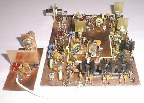
In this picture, the parallel 2N2222A transistors used for the final amplfier array are in place, along with the last of the r.f. switched T/R switched just to the left of the finals. The transmit low pass filter was constructed on a separate substrate since there was insufficient space left for this portion of the circuitry.

Here the transverter is essentially done. Note the additional 2 transistors in the middle area of the main substrate. These are the r.f. switch that controls the Vcc supply voltage to the class A amplifiers, so that their noise doesn't mask the receive signal. Before this circuitry was added, signals below about S9 could not be heard. The output low pass filter can be seen mounted to the back of the chassis, along with the fuse holder, power jack, and the transceiver connector, now removed from the substrate of earlier pictures.

Next to last picture showing some additional details. The attenuator resistors have been replaced with single units, the back panel wiring is in place, and the labelling on the front panel is done. The homebrew heatsinks have also been replaced with commercial units, mostly for esthetics. The case used is a TenTec TP-47 painted light grey. The cover half is painted flat black.

Back to the "2N2/6" page