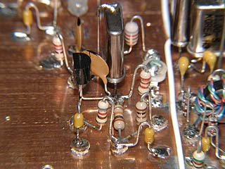
The transmit strip began with the construction of the transmit local oscillator. This circuitry is positioned inboard of the product detector.
Next, the circuitry for the transmit mixer was added. The white coax coming in from the top of this image carries the VFO signal to this stage.
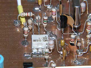
Looking from the opposite direction, one can see the two stage cascode RF amplifier components. The input tuned circuit is on the left with the output tuned circuit being on the right. A 50 Ohm trimmer controls the power level to the driver stage which was built next.
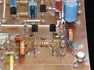
Components for the driver stage were then added. The 2N2222A uses a finned heat sink to keep it cool.
This view is from the back of the substrate; the cascode amplifier just shown is to the right.
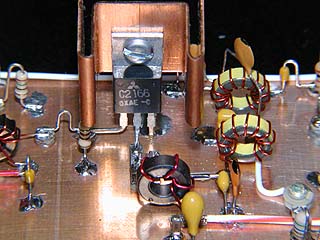
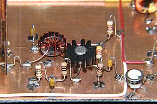
Shown here are the final amplifier and output low pass filter components. The heat sink on the 2SC2166 transistor was replaced when the completed board was packaged.
This view is from the front of the substrate; the driver stage just shown is to the left.

Completing the transmit strip are the few components which make up the receive/transmit switch.
This single transistor stage causes the 2N2/20 to transmit when the key is pressed, and at the same time attenuates the input to the receiver. It also does the shaping of the keying waveforms.

Completed 2N2/20 before
rebuilding the receive RF amplifier, and adding the board mounted RIT components.
Before packaging the rig, two additional control modules had to be built.
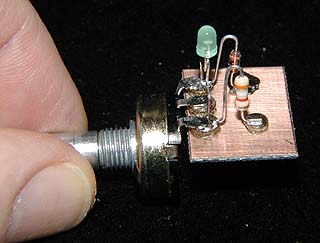
This is the receiver RF gain control module which is constructed on a small piece of PC board material. It mounts to the front panel using the potentiometer threads. Only dc voltages are controlled by this module.
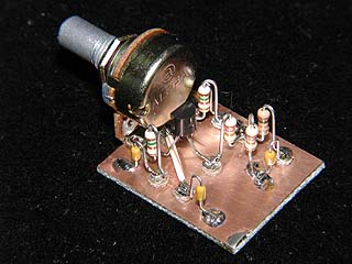
In a similar format, the receiver incremental tuning (RIT) control module was built. It too only provides dc voltages to the controlled circuitry. Those parts are mounted on the main substrate adjacent to the VFO.
This module version was built using all leaded components; the one for the 2N2/30 is all surface mount components.
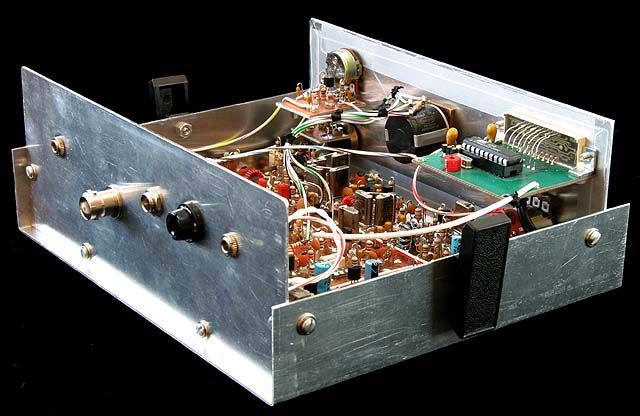
One of the items not shown
in detail is the use of a KD1JV display module to read out the operating
frequency. That module is in the upper right of this image. Its input is
connected to the VFO line driving the transmit mixer and coupled through
a 2 pF ceramic capacitor. Similar modules are also available from AADE. Both
vendors can be found on the web.
The RIT and RF gain modules, mounted to the front panel, can be seen on the upper left in this image.
Rear panel connectors from left to right include: key, antenna, power, and audio. Adjacent to the power connector is a fuse holder.
The RIT and RF gain modules, mounted to the front panel, can be seen on the upper left in this image.
Rear panel connectors from left to right include: key, antenna, power, and audio. Adjacent to the power connector is a fuse holder.
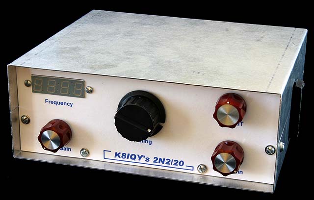
One last image of the rig
showing the front panel controls. Beginning at the left: audio gain, tuning,
RIT (upper) and RF gain (lower).
The two-piece case was bent on a 12 inch Harbor Freight brake/shear from 0.040 inch 6061 T6 aluminum sheet stock.
Lettering was printed on plain white paper, which was then affixed to adheasive backed transparent film. The edges of the film wrap around the edges of the front panel, and the controls keep the "sandwich" tight against the panel face.
Back to the "Pictures" page